Friday, June 5, 2009

Digital Visitor Counter


Digital visitor counter is a reliable circuit that takes over the task of counting Number of Persons/ Visitors in the Room very accurately. When anybody enters into the Room then the Counter is Incremented by one and when any one leaves the room then the Counter is Decremented by One. The total number of Persons inside the Room is displayed on the seven segment displays.
The microprocessor do the above job it receives the signals from the sensors, and this signals operated under the control of software which is stored in the Memory. The sensors are made with help of LDRs which are Light Dependent Resistors, whose Resistance is inversely proportional to the Light falling on it. The Laser Torch is used as the Light source and it is focused on the LDRs, the Microprocessor continuously watches the LDRs.

Digital gates Emulator


This project “Digital gates Emulator” is used to emulate the basic gates such us NOT, OR, AND. The system has the selector switch by which we can select any gate. The system has two inputs and one output. We use two SPDT switches for the inputs and for the output we use an LED. The gate selection can be done by the selector switch and it is also indicated on separate LED’s. There are three LED’s provided on the board for the gates NOT, OR, AND. The corresponding LED will glow for the corresponding gate. The main operation is done by the Microprocessor through its ports using the PPI (Programmable Peripheral Interface) IC8255. The microprocessor gets the input through the ports and it will produce the output according to the gate selected.

Automatic Plant Irrigator


The Project presented here waters our plants regularly when you are out for vocation. The circuit comprises of sensor parts built using op-amp IC LM324. Op-amp’s are configured here as a comparator. Two stiff copper wires (for one sensor) are inserte The Project presented here waters our plants regularly when you are out for vocation. The circuit comprises of sensor parts built using op-amp IC LM324. Op-amp’s are configured here as a comparator. Two stiff copper wires (for one sensor) are inserted in the soil to sense the whether the Soil is wet or dry. The Microprocessor was used to control the whole system. It monitors the sensors through the programmable peripheral interface (PPI) IC 8255. When more than two sensors sense the dry condition, then the Microprocessor will switch on the motor and it will switch off the motor when all the sensors goes wet. The Microprocessor does the above job by receiving the signals from the sensors through the PPI, and this signals operated under the control of software which is stored in ROM. We are using the 8 bit Microprocessor 8055 and the programmable peripheral interface IC 8255.d in the soil to sense the whether the Soil is wet or dry. The Microprocessor was used to control the whole system. It monitors the sensors through the programmable peripheral interface (PPI) IC 8255. When more than two sensors sense the dry condition, then the Microprocessor will switch on the motor and it will switch off the motor when all the sensors goes wet. The Microprocessor does the above job by receiving the signals from the sensors through the PPI, and this signals operated under the control of software which is stored in ROM. We are using the 8 bit Microprocessor 8055 and the programmable peripheral interface IC 8255.


Automatic Night Lamp with Morning Alarm


This Project “Automatic Night Lamp with Morning Alarm” was developed using Microprocessor. It is the Heart of the system. The sensors are made with help of LDR which are Light Dependent Resistors, whose Resistance is inversely proportional to the Light falling on it. The LDR converts the light energy into electrical energy and this variable electrical energy was converted into digital signal (0 or 1) by using the timer IC555. The Timer IC output goes low when light falls on the LDR and the timer IC output goes high when the LDR was placed in dark.

Wednesday, June 3, 2009

Access Control System


This project Access Control System is used in the places where we need more security. It can also used to secure lockers and other protective doors. The system comprises a number keypad and the keypads are connected to the 8 bit microprocessor 8085 through the programmable peripheral IC 8255. This is one of the popular microprocessor.
The microprocessor continuously monitor the keypad and if somebody enters the password it will check the entered password with the password which was stored in the memory and if it they are same then the microprocessor will switch on the device.
In our Project we are controlling a electrical device. The password can be an four digit number. If we enter the correct password then the microprocessor will switch on the load. If we want to switch off the load simply press the digit 0 in the keypad.

Saturday, May 30, 2009

Write a program to shift an eight bit data four bits right. Assume that data is in register C.

Source program:

MOV A, C
RAR
RAR
RAR
RAR
MOV C, A
HLT

Statement:Write a program to shift a 16 bit data, 1 bit right. Assume that data is in BC register pair.

Source program:
MOV A, B
RAR
MOV B, A
MOV A, C
RAR
MOV C, A
HLT


Thursday, May 28, 2009

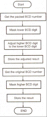
Two digit BCD number is stored in memory location 4200H. Unpack the BCD number and store the two digits in memory locations 4300H and 4301H such that


Sample problem

(4200H) = 58
Result = (4300H) = 08 and
(4301H) = 05
Source program

LDA 4200H : Get the packed BCD number
ANI FOH : Mask lower nibble
RRC
RRC
RRC
RRC : Adjust higher BCD digit as a lower digit
STA 4301H : Store the partial result
LDA 4200H : .Get the original BCD number
ANI OFH : Mask higher nibble
STA 4201H : Store the result
HLT : Terminate program execution

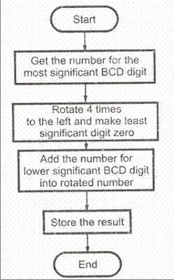
Pack the two unpacked BCD numbers stored in memory locations 4200H and 4201H and store result in memory location 4300H. Assume the least significant d


Sample problem:
(4200H) = 04
(4201H) = 09
Result = (4300H) = 94


Source program

LDA 4201H : Get the Most significant BCD digit
RLC
RLC
RLC
RLC : Adjust the position of the second digit (09 is changed to 90)
ANI FOH : Make least significant BCD digit zero
MOV C, A : store the partial result
LDA 4200H : Get the lower BCD digit
ADD C : Add lower BCD digit
STA 4300H : Store the result
HLT : Terminate program execution

Find the 2's complement of the number stored at memory location 4200H and store the complemented number at memory location 4300H.


Sample problem:

(4200H) = 55H
Result = (4300H) = AAH + 1 = ABH

Source program:

LDA 4200H : Get the number
CMA : Complement the number
ADI, 01 H : Add one in the number
STA 4300H : Store the result
HLT : Terminate program execution

Find the l's complement of the number stored at memory location 4400H and store the complemented number at memory location 4300H.


Sample problem:

(4400H) = 55H
Result = (4300B) = AAB
Source program:

LDA 4400B : Get the number
CMA : Complement number
STA 4300H : Store the result
HLT : Terminate program execution

Subtract the 16-bit number in memory locations 4002H and 4003H from the 16-bit number in memory locations 4000H and 4001H. The most significant eight


Sample problem

(4000H) = 19H
(400IH) = 6AH
(4004H) = I5H (4003H) = 5CH
Result = 6A19H - 5C15H = OE04H
(4004H) = 04H
(4005H) = OEH

Source program:

LHLD 4000H : Get first 16-bit number in HL
XCHG : Save first 16-bit number in DE
LHLD 4002H : Get second 16-bit number in HL
MOV A, E : Get lower byte of the first number
SUB L : Subtract lower byte of the second number
MOV L, A : Store the result in L register
MOV A, D : Get higher byte of the first number
SBB H : Subtract higher byte of second number with borrow
MOV H, A : Store l6-bit result in memory locations 4004H and 4005H.
SHLD 4004H : Store l6-bit result in memory locations 4004H and 4005H.
HLT : Terminate program execution.


Sunday, May 24, 2009

Statement: Add the 16-bit number in memory locations 4000H and 4001H to the 16-bit number in memory locations 4002H and 4003H. The most significant ei


Program - 5.a: Add two 16-bit numbers - Source Program 1

Sample problem:

(4000H) = 15H
(4001H) = 1CH
(4002H) = B7H
(4003H) = 5AH
Result = 1C15 + 5AB7H = 76CCH
(4004H) = CCH


Source Program 1:

LHLD 4000H : Get first I6-bit number in HL
XCHG : Save first I6-bit number in DE
LHLD 4002H : Get second I6-bit number in HL
MOV A, E : Get lower byte of the first number
ADD L : Add lower byte of the second number
MOV L, A : Store result in L register
MOV A, D : Get higher byte of the first number
ADC H : Add higher byte of the second number with CARRY
MOV H, A : Store result in H register
SHLD 4004H : Store I6-bit result in memory locations 4004H and 4005H.
HLT : Terminate program execution


Program - 5b: Add two 16-bit numbers - Source Program 2

Source program 2:
LHLD 4000H : Get first I6-bit number
XCHG : Save first I6-bit number in DE
LHLD 4002H : Get second I6-bit number in HL
DAD D : Add DE and HL
SHLD 4004H : Store I6-bit result in memory locations 4004H and 4005H.
HLT : Terminate program execution


Saturday, May 23, 2009

Statement: Add the contents of memory locations 4000H and 4001H and place the result in memory location 4002H.


Sample problem

(4000H) = 14H
(4001H) = 89H
Result = 14H + 89H = 9DH

Source program

LXI H 4000H : HL points 4000H
MOV A, M : Get first operand
INX H : HL points 4001H
ADD M : Add second operand
INX H : HL points 4002H
MOV M, A : Store result at 4002H
HLT : Terminate program execution


Statement: Exchange the contents of memory locations 2000H and 4000H

Program 1:

LDA 2000H : Get the contents of memory location 2000H into accumulator
MOV B, A : Save the contents into B register
LDA 4000H : Get the contents of memory location 4000Hinto accumulator
STA 2000H : Store the contents of accumulator at address 2000H
MOV A, B : Get the saved contents back into A register
STA 4000H : Store the contents of accumulator at address 4000H

Program 2:
LXI H 2000H : Initialize HL register pair as a pointer to memory location 2000H.
LXI D 4000H : Initialize DE register pair as a pointer to memory location 4000H.
MOV B, M : Get the contents of memory location 2000H into B register.
LDAX D : Get the contents of memory location 4000H into A register.
MOV M, A : Store the contents of A register into memory location 2000H.
MOV A, B : Copy the contents of B register into accumulator.
STAX D : Store the contents of A register into memory location 4000H.
HLT : Terminate program execution.

In Program 1, direct addressing instructions are used, whereas in Program 2, indirect addressing instructions are used.

Statement: Store the data byte 32H into memory location 4000H.

Program 1:

MVI A, 52H : Store 32H in the accumulator
STA 4000H : Copy accumulator contents at address 4000H
HLT : Terminate program execution

Program 2:

LXI H : Load HL with 4000H
MVI M : Store 32H in memory location pointed by HL register pair (4000H)
HLT : Terminate program execution

Monday, May 18, 2009

Intel 8085 microprocessor architecture

Memory

Program, data and stack memories occupy the same memory space. The total addressable memory size is 64 KB.

Program memory - program can be located anywhere in memory. Jump, branch and call instructions use 16-bit addresses, i.e. they can be used to jump/branch anywhere within 64 KB. All jump/branch instructions use absolute addressing.

Data memory - the processor always uses 16-bit addresses so that data can be placed anywhere.

Stack memory is limited only by the size of memory. Stack grows downward.


Interrupts

The processor has 5 interrupts. They are presented below in the order of their priority (from lowest to highest):

INTR is maskable 8080A compatible interrupt. When the interrupt occurs the processor fetches from the bus one instruction, usually one of these instructions:

  • One of the 8 RST instructions (RST0 - RST7). The processor saves current program counter into stack and branches to memory location N * 8 (where N is a 3-bit number from 0 to 7 supplied with the RST instruction).
  • CALL instruction (3 byte instruction). The processor calls the subroutine, address of which is specified in the second and third bytes of the instruction.

RST5.5 is a maskable interrupt. When this interrupt is received the processor saves the contents of the PC register into stack and branches to 2Ch (hexadecimal) address.

RST6.5 is a maskable interrupt. When this interrupt is received the processor saves the contents of the PC register into stack and branches to 34h (hexadecimal) address.

RST7.5 is a maskable interrupt. When this interrupt is received the processor saves the contents of the PC register into stack and branches to 3Ch (hexadecimal) address.

Trap is a non-maskable interrupt. When this interrupt is received the processor saves the contents of the PC register into stack and branches to 24h (hexadecimal) address.

All maskable interrupts can be enabled or disabled using EI and DI instructions. RST 5.5, RST6.5 and RST7.5 interrupts can be enabled or disabled individually using SIM instruction.


First 64 bytes in a zero memory page should be reserved for vectors used by RST instructions.


I/O ports

256 Input ports
256 Output ports

Registers

Accumulator or A register is an 8-bit register used for arithmetic, logic, I/O and load/store operations.

Flag is an 8-bit register containing 5 1-bit flags:

  • Sign - set if the most significant bit of the result is set.
  • Zero - set if the result is zero.
  • Auxiliary carry - set if there was a carry out from bit 3 to bit 4 of the result.
  • Parity - set if the parity (the number of set bits in the result) is even.
  • Carry - set if there was a carry during addition, or borrow during subtraction/comparison.

General registers:

  • 8-bit B and 8-bit C registers can be used as one 16-bit BC register pair. When used as a pair the C register contains low-order byte. Some instructions may use BC register as a data pointer.
  • 8-bit D and 8-bit E registers can be used as one 16-bit DE register pair. When used as a pair the E register contains low-order byte. Some instructions may use DE register as a data pointer.
  • 8-bit H and 8-bit L registers can be used as one 16-bit HL register pair. When used as a pair the L register contains low-order byte. HL register usually contains a data pointer used to reference memory addresses.

Stack pointer is a 16 bit register. This register is always incremented/decremented by 2.

Program counter is a 16-bit register.

Instruction Set

8085 instruction set consists of the following instructions:

  • Data moving instructions.
  • Arithmetic - add, subtract, increment and decrement.
  • Logic - AND, OR, XOR and rotate.
  • Control transfer - conditional, unconditional, call subroutine, return from subroutine and restarts.
  • Input/Output instructions.
  • Other - setting/clearing flag bits, enabling/disabling interrupts, stack operations, etc.
Addressing modes

Register - references the data in a register or in a register pair.
Register indirect - instruction specifies register pair containing address, where the data is located.
Direct.
Immediate - 8 or 16-bit data.


Types of Microprocessors

Types of Microprocessors according to there emergence are

Complex Instruction Set Computer (CISC)

Where most of the work is to perform by Microprocessor itself, the philosophy reduced the Line of Codes or instruction and burden processor to perform most of the task. CISC architecture was first used by Digital Equipment Corporation PDP 11 family of minicomputers.

Reduced Instruction Set Computer (RISC)

Where most of the work is to perform by the software itself, the load on a processor is very low and hence it is called future processors. The RISC architecture was used by Apple Corporation's Macintosh computers, IBM's RISC System/6000 workstations and Sun Microsystems's SPARC.

Very Long Instruction Word (VLIW)

In this architecture a compiler breaks instruction into basic operations to be performed by processor. VLIW is the next step of RISC. In this philosophy complication is moved from the hardware to the software so it reduces the hardware cost.

Superscalar Processors

They are competent of performing more than one instruction in each cycle. In this philosophy concept of cache, parallel processing and floating point were introduced.
Few other are
General Purpose Processor (GPP)
Special Purpose Processor (SPP)
Application-Specific Integrated Circuit (ASIC)
Application-Specific Instruction-set Processor (ASIP)
Digital Signal Processor (DSP)

Intel processor

Processors mainly have two parameters: width of microprocessor and speed. Speed is calculated in Megahertz (MHz).The width of the processor can be expressed in the form of Internal Register, I/O bus and memory address bus. Microprocessor has different types; Intel processor, AMD, Cyrix, NexGen, IDT, Rise Processors.

Intel processor that belongs to the First Generation of Processors is 8088, 8086, 80186, 80188, and 8087. Intel processors 286, 80287 belong to Second Generation of Processors.

Third Generation microprocessor are 386SX, 386SL, 386DX. AMD 486 (5x86), Cyrix/TI. 486, 486SX, 486SX2, 487SX, 486SL, 486SL2, 486DX, 486DX2, 486DX4 belongs to the Fourth Generation of Microprocessor. Other different types of microprocessor are 486Pentium OD, Pentium 60/66, Pentium 75–200, Pentium MMX, Pentium Pro, Pentium II, Pentium II PE, Celeron, Celeron A, Celeron III, Pentium III, Pentium IIIE, Pentium Xeon, Pentium IIIE Xeon, AMD K5, AMD K6, AMD K6-2, AMD K6-3, AMD Athlon, AMD Duron, AMD Athlon 4 (Thunderbird), AMD Athlon 64 and 64 FX,Cyrix 6x8, Cyrix 6x86MX/MII, Cyrix III, NexGen Nx586, IDT Winchip, IDT Winchip2/2A.

Saturday, May 16, 2009

Microprocessor Progression: Intel

­ The computer you are using to read this page uses a microprocessor to do its work. The microprocessor is the heart of any normal computer, whether it is a desktop machine, a server or a laptop. The microprocessor you are using might be a Pentium, a K6, a PowerPC, a Sparc or any of the many other brands and types of microprocessors, but they all do approximately the same thing in approximately the same way.

A microprocessor -- also known as a CPU or central processing unit -- is a complete computation engine that is fabricated on a single chip. The first microprocessor was the Intel 4004, introduced in 1971. The 4004 was not very powerful -- all it could do was add and subtract, and it could only do that 4 bits at a time. But it was amazing that everything was on one chip. Prior to the 4004, engineers built computers either from collections of chips or from discrete components (transistors wired one at a time). The 4004 powered one of the first portable electronic calculators.


­ If you have ever wondered what the microprocessor in your computer is doing, or if you have ever wondered about the differences between types of microprocessors, then read on. In this article, you will learn how fairly simple digital logic techniques allow a computer to do its job, whether its playing a game or spell checking a document!


The first microprocessor to make it into a home computer was the Intel 8080, a complete 8-bit computer on one chip, introduced in 1974. The first microprocessor to make a real splash in the market was the Intel 8088, introduced in 1979 and incorporated into the IBM PC (which first appeared around 1982). If you are familiar with the PC market and its history, you know that the PC market moved from the 8088 to the 80286 to the 80386 to the 80486 to the Pentium to the Pentium II to the Pentium III to the Pentium 4. All of these microprocessors are made by Intel and all of them are improvements on the basic design of the 8088. The Pentium 4 can execute any piece of code that ran on the original 8088, but it does it about 5,000 times faster!

The following table helps you to understand the differences between the different processors that Intel has introduced over the years.

Name
Date
Transistors
Microns
Clock speed
Data width
MIPS
8080
1974
6,000
6
2 MHz
8 bits
0.64
8088
1979
29,000
3
5 MHz
16 bits
8-bit bus
0.33
80286
1982
134,000
1.5
6 MHz
16 bits
1
80386
1985
275,000
1.5
16 MHz
32 bits
5
80486
1989
1,200,000
1
25 MHz
32 bits
20
Pentium
1993
3,100,000
0.8
60 MHz
32 bits
64-bit bus
100
Pentium II
1997
7,500,000
0.35
233 MHz
32 bits
64-bit bus
~300
Pentium III
1999
9,500,000
0.25
450 MHz
32 bits
64-bit bus
~510
Pentium 4
2000
42,000,000
0.18
1.5 GHz
32 bits
64-bit bus
~1,700
Pentium 4 "Prescott"
2004
125,000,000
0.09
3.6 GHz
32 bits
64-bit bus
~7,000

Compiled from The Intel Microprocessor Quick Reference Guide and TSCP Benchmark Scores

Information about this table:

    What's a Chip?
    A chip is also called an integrated circuit. Generally it is a small, thin piece of silicon onto which the transistors making up the microprocessor have been etched. A chip might be as large as an inch on a side and can contain tens of millions of transistors. Simpler processors might consist of a few thousand transistors etched onto a chip just a few millimeters square.

  • The date is the year that the processor was first introduced. Many processors are re-introduced at higher clock speeds for many years after the original release date.
  • Transistors is the number of transistors on the chip. You can see that the number of transistors on a single chip has risen steadily over the years.
  • Microns is the width, in microns, of the smallest wire on the chip. For comparison, a human hair is 100 microns thick. As the feature size on the chip goes down, the number of transistors rises.
  • Clock speed is the maximum rate that the chip can be clocked at. Clock speed will make more sense in the next section.
  • Data Width is the width of the ALU. An 8-bit ALU can add/subtract/multiply/etc. two 8-bit numbers, while a 32-bit ALU can manipulate 32-bit numbers. An 8-bit ALU would have to execute four instructions to add two 32-bit numbers, while a 32-bit ALU can do it in one instruction. In many cases, the external data bus is the same width as the ALU, but not always. The 8088 had a 16-bit ALU and an 8-bit bus, while the modern Pentiums fetch data 64 bits at a time for their 32-bit ALUs.
  • MIPS stands for "millions of instructions per second" and is a rough measure of the performance of a CPU. Modern CPUs can do so many different things that MIPS ratings lose a lot of their meaning, but you can get a general sense of the relative power of the CPUs from this column.
From this table you can see that, in general, there is a relationship between clock speed and MIPS. The maximum clock speed is a function of the manufacturing process and delays within the chip. There is also a relationship between the number of transistors and MIPS. For example, the 8088 clocked at 5 MHz but only executed at 0.33 MIPS (about one instruction per 15 clock cycles). Modern processors can often execute at a rate of two instructions per clock cycle. That improvement is directly related to the number of transistors on the chip and will make more sense in the next section.